Active OLED

Active OLED Function

Active-Matrix Organic Light Emitting Diode ("AMOLED") Displays function with separated logical and power drive methods. The logic drive is controlled by an integrated display driver ASIC. The power drive to each pixel is isolated utilizing a Thin-Film Transistor ("TFT") layer to the structure

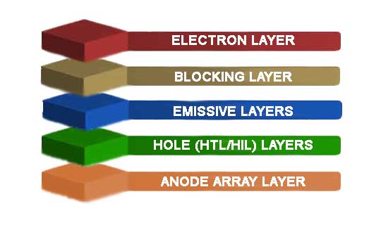
The anode and cathodes are arranged in perpendicular arrays on the top and bottom layers. The Electron Transport Layer ("ETL") facilitates the charge carrying electrons from the cathode. The Blocking Layer ("BL") is used to contain electrons towards the Emissive Layer ("EL"). The EL is a series of Positive & Negative material deposits ("P-N") that with current drive emit light. The Hole Transport Layer ("HTL") receives holes from the emissive layer and the corresponding Hole Injection Layer ("HIL") receives the holes from the Anode.

Material Layers

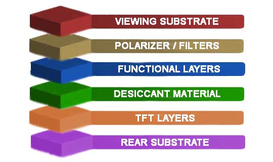
An AMOLED Display will consist primarily utilizing glass substrate. Flexible OLED will substitute Polyethylene Terephthalate ("PET") thin films as a substrate material. PET materials while manufacturing will still utilize glass substrate carriers and be separated at the end of the encapsulation process.

The aforementioned functional layers will be deposited on the substrate already integrated with a TFT layer. Since OLED materials deteriorate by moisture, a desiccant layer is added to control inherent moisture from the manufacturing process. A rear encapsulation layer of glass or metal will be sealed to the substrate to fully contain the deposited layers and desiccant from the outside environment. Light polarizing thin films and in some module cases a color filter layer may be utilized to colorize white illumination if the color emission requires.

Photolithography

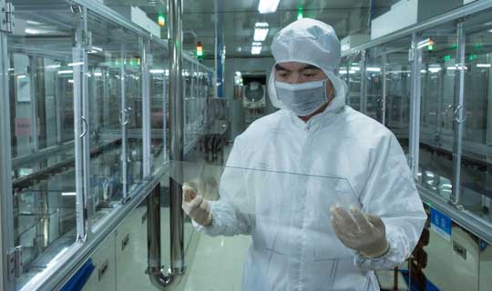
Photolithography is a common process for optical electronics of putting transparent circuitry on glass substrate. The circuit is a fine layer of Indium Tin Oxide ("ITO") which serves as conductive electrodes on the glass with minimal observability. The process is performed in a cleanroom under light-sensitive conditions. The general process includes application of photoresist to determine where ITO is allowed, controlled exposure and development baking stage, and removal of the photoresist materials. There are many cleaning stages throughout this process.

Vacuum Deposition

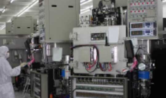
Vacuum Deposition is a thermal evaporation process performed in a vacuum environment. The process allows high purity of intended deposit material without solvents or moisture which is detrimental to the OLED emissive layer.

The common materials for the emissive layer include organometallic chelates and various OLED dopants dyes or dendrimers that determine the specific light wavelength emission profiles of the emission.

The vapor is masked on the substrate in the deposition phase to control the pattern. Multi-color or full-color designs may repeat sequential deposition phases for each emissive color.

IC Bonding

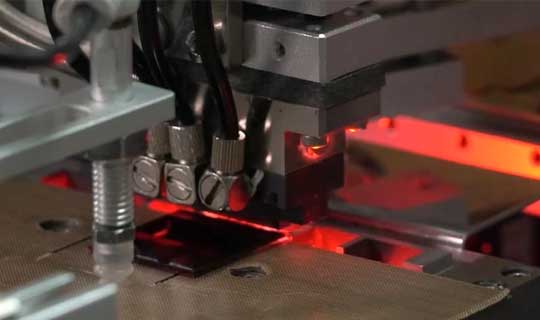
OLED products will have substantial quantities of pixels or segments to multiplex. Modules will incorporate an application-specific integrated circuit ("ASIC"), commonly just referred to as the display driver IC. These ICs must be paired to provide the correct number of segments & commons for drive of the panel and equally provide the correct power and drive techniques for a current-driven technology like OLED material. Display drivers can support various interface protocols and standards. These semiconductors can be bonded by Chip-On-Glass ("COG") or Chip-On-Flex ("COF") bonding methods. Most ICs are migrating towards compact COG driver packages for cost efficiency, but some aspect ratios and resolution may require COF packaged ICs for impedance matching of the panel impacting panel uniformity, or "mura" a common Japanese terminology from the display industry referring to the unevenness of light emission.

Interconnect Bonding

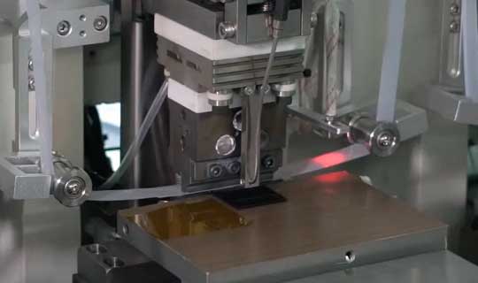
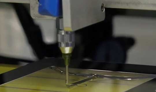
OLED solutions may have various interconnection options for your system. Most designs will natively will be designed for a bonded interconnection option such as flexible printed circuit ("FPC"). Flex-to-glass bonding is accomplished with Anisotropic Conductive Film ("ACF") that is a durable conductive adhesive between the glass and film attachment area. After bonding, it is common for electrical insulation, limiting environmental exposure, and strain relief material to be applied over the bond area on the glass and FPC. Common material for securing the bond area include Room Temperature Vulcanized ("RTV") silicone which allows for improved quality in storage, handling, and subsequent module integration processes. These interconnects may be customized for specific pin assignments and consolidation of interconnection with touchscreen overlays.

Touchscreen Bonding

OLED Displays can also be bonded with OSD's touch and lens products. Select OLED products may offer on-cell touch sensors natively and simply only require a cover lens to be added. Solutions without touch function can be paired with touchscreens or lenses utilizing various bonding methods.

Double-Sided Tape ("DST") which is bonding only the perimeter and leaves a small air void is an economical option. Additionally there are options for optical bonding including film-type optically-clear adhesive ("OCA"), liquid optical-clear adhesive ("LOCA"), and solid clear adhesive ("SCA") methods. These optical bonding methods have no air void between the display and bonded overlay providing optimal clarity and optics.

Quality & Packaging

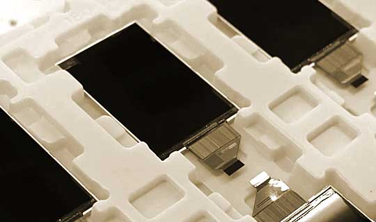
OSD Performs 100% inspection on all OLED modules including cosmetic, functional, and conformance tests. We maintain a continuous-improvement quality system compatible with our ISO certifications. We additionally are able to cooperate with customers implementing specific test fixtures, or standards, agreed in specification. Protective packaging can be either standard or customized custom designed for OLEDs and OSD is able to work with our customers to meet packaging, labeling, and logistical requirements . OLED packaging is also sealed with additional large desiccants for improved storage protection.

OSD is able to accommodate customer-specified cartons, trays, carton labels with customized inventory management labels, and other packaging elements to integrate with the customer's supply chain and inventory management systems.