Touchscreens

PCAP SITO Structure

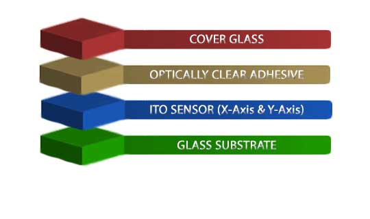
A Single Indium Tin Oxide ("SITO") touch sensor stack has a single ITO layer with the X-Y pattern, usually a diamond pattern, on the top surface of the substrate (glass or film). The patterning has cross bridges made of conductive and insulating materials allowing the X-Y electrodes to cross on the same layer of the substrate. This design eliminates the second layer of ITO present in DITO touch panel stacks and reduces the channel-routing margin outside the active area.

This is one of the most effective PCAP stack-ups, as it offers a high degree of accuracy as well as more control of charge time and sensitivity. SITO touch panels are the preferred solution for applications requiring high sensitivity control, rugged environments, touch surface moisture, glove usage, or stylus implementations.

PCAP DITO Structure

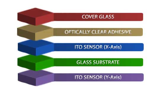
A Double-Sided Indium Tin Oxide ("DITO") stack has ITO layers on different sides of a glass or film substrate, with Y-patterning on the top sensing surface, and X patterning is on the bottom surface. The primary advantage of DITO is production and material simplicity resulting in a lower-cost solution respectively. DITO has high quality, resolution, durability, and functionality for most general purpose applications that do not require specialized sensitivity profiles for demanding environments or environmental conditions.

Photolithography

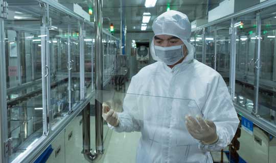
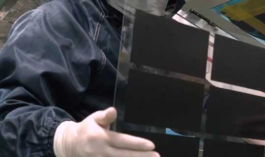
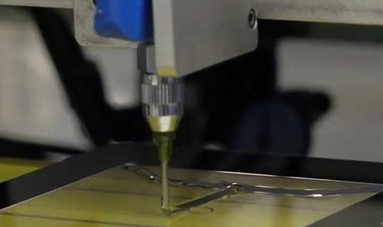
Photolithography is a common process for optical electronics of putting transparent circuitry on glass substrate. The circuit is a fine layer of Indium Tin Oxide ("ITO") which serves as conductive circuit on the glass with minimal observability. The process is performed in a cleanroom under light-sensitive conditions. The general process includes application of photoresist to determine where ITO is allowed, controlled exposure and development baking stage, and removal of the photoresist materials. There are many cleaning stages throughout this process. Patterns on the glass for touch sensor will comply with SITO or DITO predefined structures, mechanical dimensions, sense lines, and interconnect locations.

Sensor Types

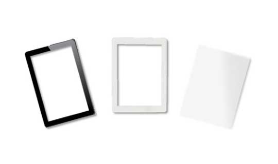
There are a few different types of touchscreen material stacks. These include Glass-on-Glass ("G+G"), Glass-on-Film ("G+F"), Glass-on-Double-Film ("G+F+F"), Glass-on-Double-Glass ("G+G+G"), and On-Glass-Solutions ("OGS").

Primary differences are the SITO and DITO structuring, number of layers, and types of substrates utilized. OGS structures are combining the capacitive sensor structure onto the display glass substrate. This solution is optimal for thin and lightweight products, but can have high costs and minimum order requirements for industrial customers if unavailable. Film substrates can offer cost savings, weight, mechanical thickness, and other considerations for some target requirements. Glass substrate is one of the most durable to the most demanding industrial environments.

Scribing

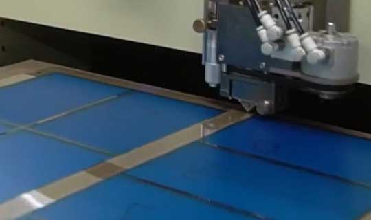
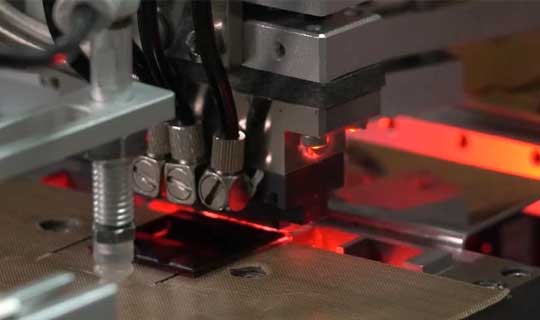
Touchscreen sensors are produced on larger substrates. The substrate size is determined by the technology and processing equipment. Smaller sensors may have higher minimum project requirements for customizations for minimum production runs and purchase multiples. The sensors will be cut (film) or scribe & break (glass) for separating the substrate to individual panel sensors. Glass and film sensors have additional processes such as edge smoothing on scribed edges (glass), film optically-clear adhesive ("OCA") layering for designs with multiple layers of film or glass, in addition to other proprietary and quality processes.

Driver Attachment

Touchscreen solutions may have various interconnection options for your system. Most designs natively will be designed for a bonded interconnection option such as flexible printed circuit ("FPC"). Flex-to-glass bonding is accomplished with Anisotropic Conductive Film ("ACF") that is a durable conductive adhesive between the glass and film attachment area. After bonding, it is common for electrical insulation, limiting environmental exposure, and strain relief material to be applied over the bond area on the glass and FPC. Common material for securing the bond area include Room Temperature Vulcanized ("RTV") silicone which allows for improved quality in storage, handling, and subsequent module integration processes. Capacitive touch panels will almost exclusively have driver ICs embedded on the FPC in close proximity to the sensor. The interconnect may be customized for various interface types like popular digital interfaces USB or I²C. Interconnects can also be customized or consolidated to displays and other user interface components for minimal assembly connections and system board connector space.

Cover Glass Lenses

Projective capacitive ("PCAP") touchscreens have sensors that are not directly contacted. These sensors will be recessed beneath glass, plastic, or other materials that don't interfere with the technology sensing. The most common applications utilize cover glass lenses. These lenses can be of various glass types, glass thickness, strengthening processes, masking, and artwork. The lenses may retain an active area for visibility to display active areas in layers below or be used without displays or illumination.

Cover glass will be bonded with optically-clear adehsive film ("OCA") with the film or glass sensors. Cover glass lenses may also seek to be oversized with perimeter adhesive or gaskets ready for system integration. For more information on OSD Displays internal glass capabilities, please visit our screen protectors section for further details.

Touchscreen Bonding

Completed touchscreens can also be bonded with OSD's display technologies. There may be multiple bonding methods available for your materials.

Double-Sided Tape ("DST") which is bonding only the perimeter and leaves a small air void between the display. This solution is the most cost-effective in materials and process, it has higher production yields for easier remedy for servicing and production non-conformity, and is sufficient for many environments.

Additionally there are options for optical bonding. These include film-type optically-clear adhesive ("OCA"), liquid optical-clear adhesive ("LOCA"), and solid clear adhesive ("SCA") types. These have no air void between the touchscreen and display assemblies providing optimal clarity and optics. OCA solutions require flush surfaces and specific materials and environments. LOCA is a resin that is applied and cured. It is able to remedy uneven surfaces bonding and it is highly durable for the most challenging environmental conditions. LOCA is not forgiving to servicing or production errors, so it has higher cost since even the most minor cosmetic imperfection can result in total loss of display and touchscreen materials. SCA is a solid material that is more alike to OCA, but has specific curing methodologies that allow servicing and production corrections to optimize yields.

Touchscreen Tuning

Capacitive touchscreens are provided with digital interface drivers included. Sensors are essentially antennas and can capture surrounding noise in addition to targeted user interaction. Modern touchscreen drivers have various levels of active noise suppression, sensitivity adjustment, and other features.

Many touch controllers support flash programming to have updated tuning profiles. Select chipsets allow for tuning profiles to be generated by our engineers.

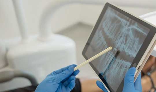
Tuning can be optimized for medical gloves, heavy work gloves, stylus usage, fresh water spray, saltwater spray, condensation and moisture, and other surrounding system or environmental noise to ensure the system remains responsive and accurate in demanding and life-critical applications.